Purpose
The RT8086B is a current mode COT step-down converter with the input voltage range from 2.8V to 5.5V and provides 3.5A outputcurrent. This document explains the function and use of the RT8086B evaluation board (EVB), and provides information to enable operation, modification of the evaluation board and circuit to suit individual requirements.
Introduction
General Product Information
The RT8086B is a high efficiency, synchronous step-down DC/DC converter. The available input voltage range is from 2.8V to 5.5V and the regulated output voltage is adjustable from 0.6V to 3.3V while delivering up to 3.5A of output current.Product Feature. The internal synchronous low on-resistance power switches increase efficiency and eliminate the need for an external Schottky diode. The current mode constant on-time operation with internal compensation allows the transient response to be optimized over a wide range of loads and output capacitors. The RT8086B is available in the UQFN-12L 2x2 (FC) package.
Product Features
-
High Efficiency Up to 95%
-
Low RDS(ON) Switches : 50mΩ/40mΩ
-
0.6V Reference Allows for Low Output Voltage
-
Internal Compensation
-
Input Voltage Range : 2.8V to 5.5V
-
Adjustable Output Voltage from 0.6V to 3.3V
-
1.2MHz Switching Frequency
-
Start-Up into Pre-Biased Load
-
Built in Soft-Start
-
Power Good Indication
-
Cycle-by-Cycle Current Limit
-
Input Under Voltage Lockout
-
Output Under Voltage Protection (Hiccup)
-
Thermal Shutdown Protection
-
RoHS Compliant and Halogen Free
Key Performance Summary Table
|
Key Features
|
Evaluation Board Number : PCB064_V1
|
|
Default Input Voltage
|
3.3V
|
|
Max Output Current
|
3.5A
|
|
Default Output Voltage
|
1.2V
|
|
Default Marking & Package Type
|
RT8086BGQUF, UQFN-12L 2x2 (FC)
|
|
Operation Frequency
|
1.2MHz Switching Frequency
|
Bench Test Setup Conditions
Headers Description and Placement
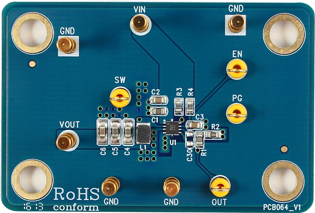
Please carefully inspect the EVB IC and external components, comparing them to the following Bill of Materials, to ensure that all components are installed and undamaged. If any components are missing or damaged during transportation, please contact the distributor or send e-mail to evb_service@richtek.com.
Test Points
The EVB is provided with the test points and pin names listed in the table below.
|
Test point/
Pin name
|
Signal
|
Comment (expected waveforms or voltage levels on test points)
|
|
PVIN
|
Input voltage
|
Power Input. The available input voltage range is from 2.8V to 5.5V. A 10µF or larger input capacitor is needed to reduce voltage spikes at the input.
|
|
PGND
|
Ground
|
Power Ground.
|
|
AGND
|
Ground
|
Analog Ground.
|
|
NC
|
No Internal Connection
|
No Internal Connection.
|
|
VOUT
|
Output Voltage
|
Sense Input Pin for Output Voltage.
|
|
FB
|
Feedback Input Voltage
|
Feedback Input. This pin used to set the output voltage of the converter to regulate to the desired value via an external resistive divider. The feedback reference voltage is 0.6V typically.
|
|
LX
|
Switch Node test pin
|
Switch Node. Output of the internal high side and low side MOSFETs.
|
|
EN
|
Enable test point
|
Enable Control Input. A logic-high (1.2V < EN < 5.5V) enables the converter; a logic-low forces the IC into shutdown mode.
|
|
PGOOD
|
PGOOD test point
|
Power Good Indicator. The output of this pin is an open drain with internal pull-up resister to VIN. The output of this pin is pulled to high when the FB voltage is within 10%; otherwise it is Low.
|
|
VIN
|
Input Voltage
|
Supply Voltage for Internal Control Circuit. It is connected to PVIN inside the chip.
|
Power-up & Measurement Procedure
1. Apply a 3.3V nominal input power supply (2.8V to 5.5V) to the VIN and GND terminals
2. Connect an external load up to 3.5A to the VOUT and GND terminals and verify the output voltage and current.
Output Voltage Setting
Set the output voltage with the resistive divider (R1, R2) between External Input and GND with the midpoint connected to VREFIN. The output is set by the following formula :

Schematic, Bill of Materials & Board Layout
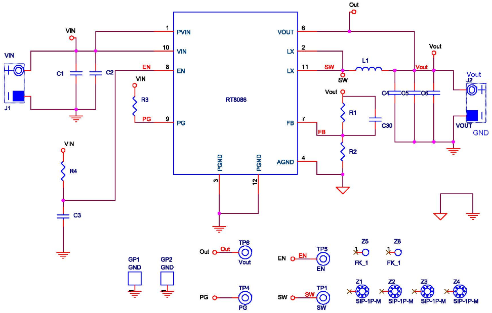
EVB Schematic Diagram
Bill of Materials
|
Reference
|
Qty
|
Part Number
|
Description
|
Package
|
Manufacture
|
|
C1
|
1
|
0603X106M6R3
|
10µF/X5R/6.3V/0603
|
C-0603
|
WALSIN
|
|
C2, C3
|
2
|
C1608X7R1H104KT000N
|
0.1µF/X7R/50V/0603
|
C-0603
|
TDK
|
|
C4, C5
|
2
|
0603X106M6R3
|
10µF/X5R/6.3V/0603
|
C-0603
|
WALSIN
|
|
C6
|
1
|
C1608X7R1H104KT000N
|
0.1µF/X7R/50V/0603
|
C-0603
|
TDK
|
|
C30
|
1
|
|
NC
|
|
|
|
GP1, GP2
|
2
|
|
GND
|
|
|
|
J1
|
1
|
|
VIN
|
|
|
|
J2
|
1
|
|
VOUT
|
|
|
|
L1
|
1
|
PIFE25201B-1R0M
|
1.0µH
|
|
Cyntec
|
|
R1, R2
|
2
|
0603 200K 1%
|
200k
|
R-0603
|
WALSIN
|
|
R3, R4
|
2
|
0603 100K 1%
|
100K
|
R-0603
|
WALSIN
|
|
TP1
|
1
|
|
SW
|
|
|
|
TP4
|
1
|
|
PG
|
|
|
|
TP5
|
1
|
|
EN
|
|
|
|
TP6
|
1
|
|
VOUT
|
|
|
|
U1
|
1
|
RT8086BGQUF
|
DC/DC Converter
|
UQFN-12L 2x2 (FC)
|
RICHTEK
|
|
Z1, Z2, Z3, Z4
|
4
|
|
SIP-1P-M
|
|
|
|
Z5, Z6
|
2
|
|
FK_1
|
|
|
PCB Layout
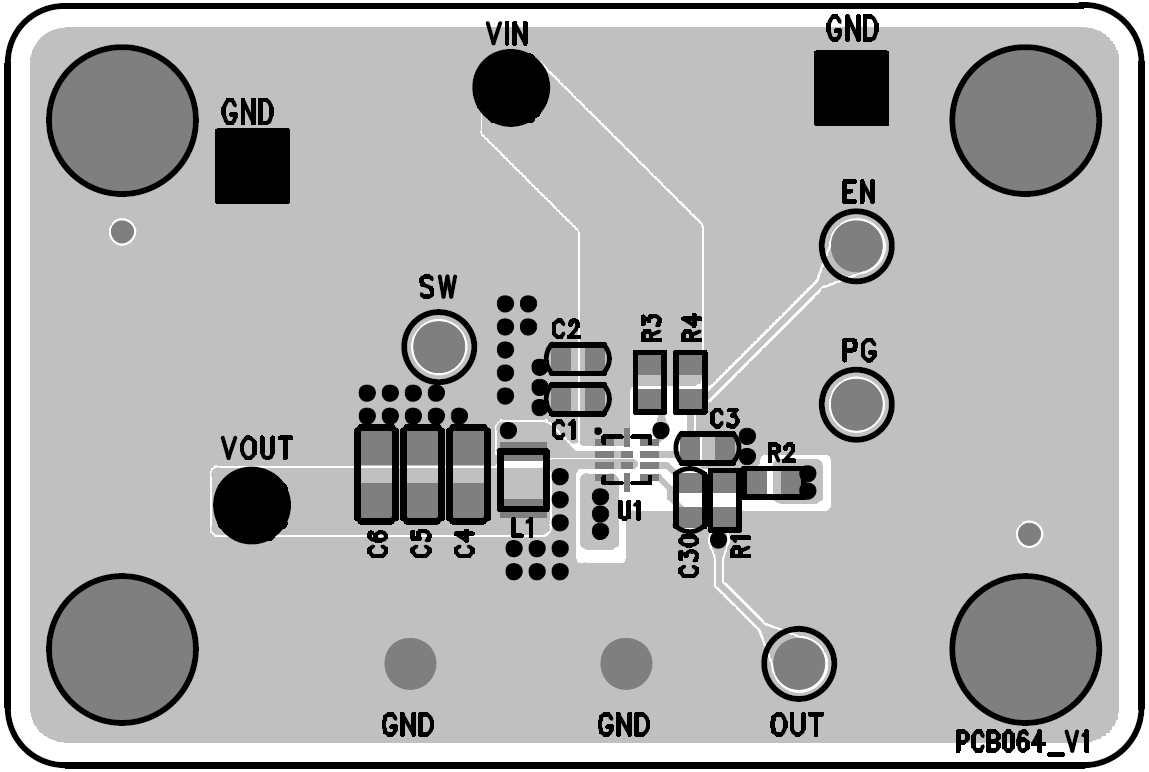
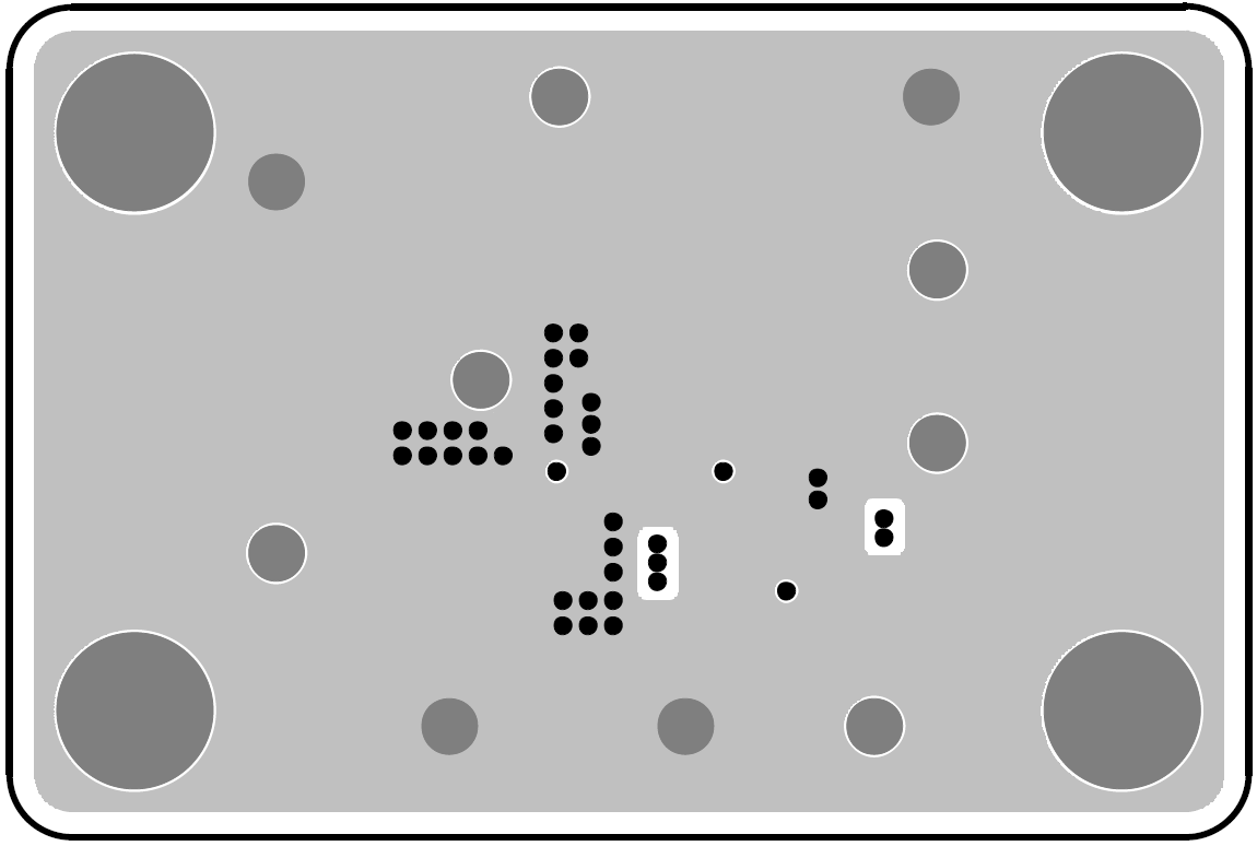
Top View (1st layer)
PCB Layout—Inner Side (2nd Layer)
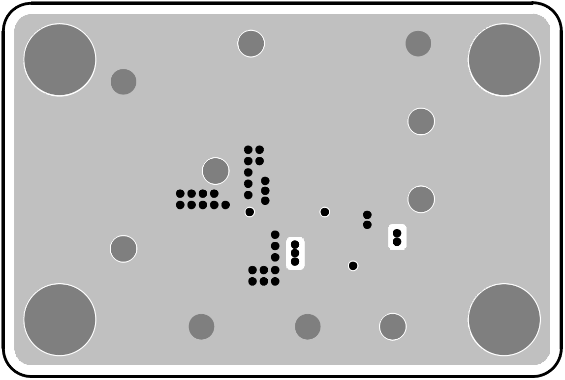
PCB Layout—Inner Side (3rd Layer)
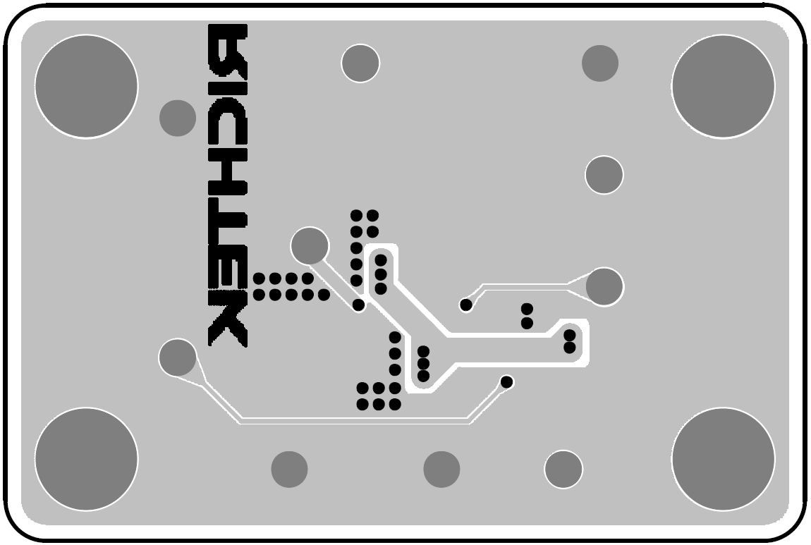
Bottom View (4th Layer)